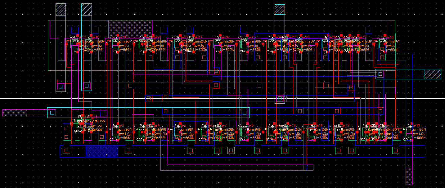
The Full Adder cell was built from a reference Static CMOS implementation schematic. That design was then converted to a minimum size layout. After a first LVS and simulation, a NAND and inverter were appended to the left side to made a full array cell and the routing was adjusted to facilitate “drop-in” layout.
Schematic

Symbol

Functional

Layout

Interconnect demonstration
Extracted
LVS

Schematic Simulation

Post-Layout (Extracted) Simulation

